Technology

MMIC Advanced Technology

WIN's technology roadmap covers both HBT and HEMT processes. More than 20 processes are available and production-ready. WIN will continue to provide various cutting-edge processes to keep our customers ahead of the game.

In addition, in terms of the breadth of the technology, the primary compound semiconductor materials have expanded from GaAs to GaN in order to satisfy the diverse wireless communication needs. In terms of market application, we have actively focused on the R&D for 5G infrastructure and optical communications technologies under the Internet of Things (IoT) trend in order to capture future market opportunities.

HBT

H02U-C4/D4/E4/F4

4th Generation HBT for GSM/3G/4G/Wi-Fi

H02U-C5/D5/F5/H5

5th Generation HBT for GSM/3G/4G/5G/Sub-6GHz/Wi-Fi/HPUE

H01U-H7/R7

7th Generation HBT for GSM/3G/4G/5G/Sub-7GHz/Wi-Fi/HPUE

pHEMT

PD50-1x/32/42

0.5μm E/D pHEMT

PD50-30

0.5μm pHEMT

PD25

0.25/0.5μm E/D pHEMT

PP50-12

0.5 μm 8V Operation pHEMT

PP25-1x

0.25μm 6V Operation pHEMT

PP15-5x/6x

0.15μm 6V Operation pHEMT

PP10-1x/2x

0.1μm 4V Operation pHEMT

PE15-0P

0.15μm E-mode 4V Operation pHEMT

PL15-1x

0.15μm 4V Operation pHEMT

PQH1-12

0.18μm 8V Operation pHEMT

PQH1-0P

0.18μm 4V Operation pHEMT

PQG3-0C

0.15μm E/D mode 4V Operation pHEMT

PINHEMT

PIH0-03

0.1μm 4V Power GaAs pHEMT with Integrated Vertical PIN and Schottky Barrier Diodes MMIC Technology

PIH1-10

Optical gate, 4V Power GaAs pHEMT with Integrated Vertical PIN and Schottky Barrier Diodes MMIC Technology

BiHEMT

PH50-C4

High efficiency HBT4 + Lower Ron pHEMT

PH50-D4

High Linearity HBT4 + Lower Ron pHEMT

GaN

NP12-01

0.12μm 28V Operation GaN HEMT

NP15-00

0.15μm 28V Operation GaN HEMT

NP25-0x/11

0.25μm 28V Operation GaN HEMT

NP25-20

0.25μm 40V Operation GaN HEMT

NP45-11

0.45μm 50V Operation GaN HEMT

IPD/PIN

IP2M-10

8V Operation IPD

IP3M-00

28V Operation IPD

IP3M-01

50V Operation IPD

PIN3-00

3μm i-layer Diode

HVD1-00

Varactor Diode

WIN provides various optional processes to fullfill various unique application requirements and package technology. That approach enables highly integrated product design and superior performance with advanced packaging.
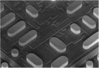
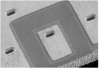
pHEMT
HBT
BiHEMT

Bump

This interconnection structure can be used for flip-chip attachment of GaAs die to a variety of substrate material.

Remark: pHEMT with EMR(Enhanced moisture ruggedness) process is required.
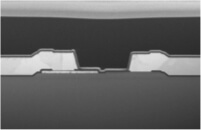
MET3

The optional metal layer for compact interconnection designs and high Q-factor inductors.
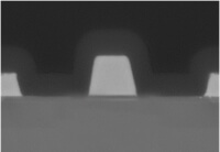
ESD Diode

The optional PN diodes for ESD protection.

0.5umE/D pHEMT devices

0.5um E/D mode for logics circuit design.
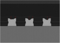
Hotvia

1. BS via could be designed as GND or for transmitting the RF signals.

2. Simple BS metal pattern for easy Installation with die attachment process.

3. Eliminate wire bonding for great RF performance.

Technology

MMIC Application Portfolio

MMIC Advanced Technology

Optoelectronic Technology Development